
Enhancing Semiconductor Stability: Vacuum Chamber Manufacturing Insights
Semiconductor equipment plays a vital role in modern technology, and one of the keys to manufacturing semiconductor equipment is the vacuum chamber. This article will comprehensively analyze the manufacturing process of vacuum chamber.
What is a vacuum chamber?
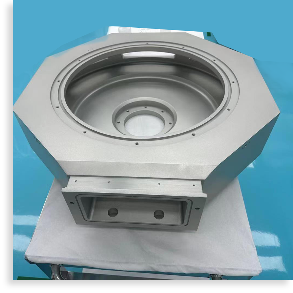
A vacuum chamber is a vacuum environment vessel used in semiconductor equipment to manufacture semiconductor chips, and its main function is to provide a stable vacuum environment for semiconductor processing. In semiconductor manufacturing, many processes need to be carried out in a vacuum or very low-pressure environment because oxygen, water vapor, dust, and other impurities in the air can negatively affect semiconductor devices. Therefore, vacuum chambers are widely used in semiconductor equipment, such as photolithography, thin film deposition equipment, and ion implantation equipment. In these devices, vacuum chambers play a key role, and their stability and precision have a significant impact on the fabrication and performance of semiconductor devices.
Manufacturing process of vacuum chamber
1.Design and Manufacturing
The manufacturing of vacuum cavities is a highly technical process that requires rigorous design and manufacturing. The manufacturing process needs to take into account factors such as the choice of material, the size of the cavity, the requirement of vacuum degree and so on. Different materials have different characteristics. When selecting materials for vacuum cavities, their physical and chemical properties, such as coefficient of thermal expansion, thermal conductivity, chemical stability and other factors, need to be considered. The commonly used materials include stainless steel, aluminum alloy, titanium alloy and so on. These materials have good mechanical properties, corrosion resistance and thermal conductivity, and are not easy to oxidize or release gases in a vacuum environment. For special requirements of semiconductor devices, such as high-frequency microwave devices and optoelectronic devices, etc., ceramic materials or semiconductor materials can also be selected.
2. Cleaning and treatment
Before manufacturing the vacuum chamber, the material needs to be cleaned and treated to ensure the purity and flatness of the chamber surface. The cleaning and treatment process requires the use of special solutions and tools.
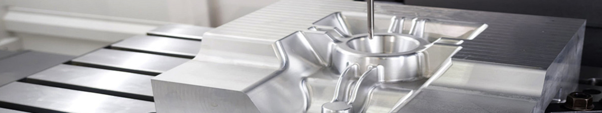
3. Processing
In terms of processing technology, attention needs to be paid to the treatment of the cavity surface to avoid defects, affecting its performance. Machining, EDM, laser processing, chemical corrosion and other methods are usually used to deal with the surface. In addition, in order to avoid impurity contamination, strict cleaning measures need to be taken during the processing.
4. Welding and assembly
 In the cleaning and processing is completed, the need for various parts of the welding and assembly. The welding and assembly process needs to pay attention to the control of temperature and pressure to avoid material deformation and air leakage phenomenon.
5. Inspection and testing
After the manufacturing is completed, the vacuum chamber needs to be inspected and tested. The inspection methods mainly include visual inspection, leakage rate test, internal cleanliness test, etc. The inspection items include vacuum degree, sealing and air leakage rate. The testing process requires the use of high-precision testing equipment and instruments.
Manufacturing a stable vacuum chamber is a crucial step in the semiconductor device production process. Only through scientific design, precise manufacturing, rigorous cleaning and processing, accurate welding and assembly, as well as thorough inspection and testing, can the quality and stability of semiconductor devices be ensured. If you require precision CNC machining and die-casting parts for the semiconductor, medical, and optical fields, please send us the drawing inquiry for further evaluation.