
Semiconductor Manufacturing’s Vacuum Chamber
In the fast-paced world of modern industry, technological innovation is a driving force that constantly shapes and reshapes our lives. Two key elements, semiconductor chambers and vacuum chambers, have become indispensable tools in the industrial landscape, particularly in semiconductor manufacturing. This article explores the critical role these chambers play in the semiconductor industry and how their integration has paved the way for groundbreaking advancements.
Semiconductor Chambers: The Heart of Microelectronics
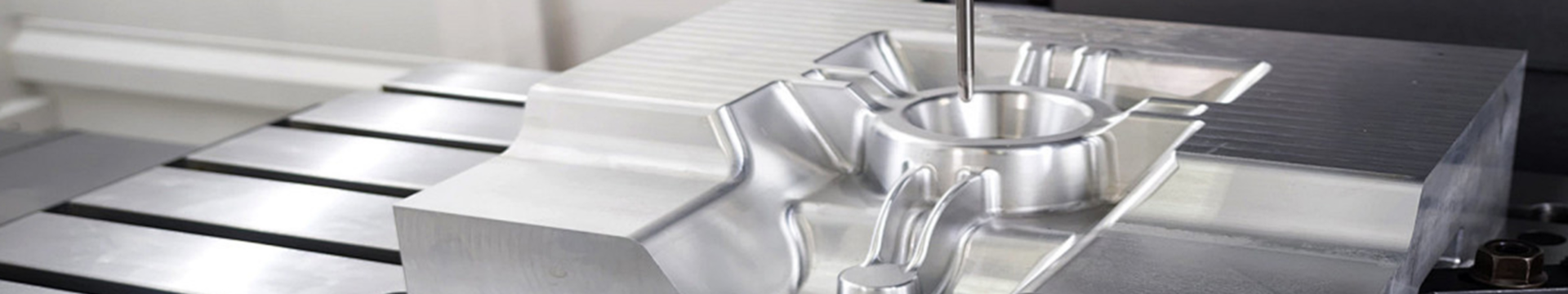
Semiconductor chambers, often referred to as process chambers, are the core components of semiconductor manufacturing equipment. These chambers are designed to precisely deposit, etch, and treat materials at the nanoscale, enabling the creation of intricate microelectronics components such as integrated circuits, microprocessors, and memory chips.
Within semiconductor chambers, various processes take place, including chemical vapor deposition (CVD), physical vapor deposition (PVD), etching, and ion implantation. These processes involve the controlled application of materials and energy to silicon wafers, enabling the creation of tiny transistors and interconnects that power our electronic devices.
Vacuum Chambers: Enabling Precision and Purity

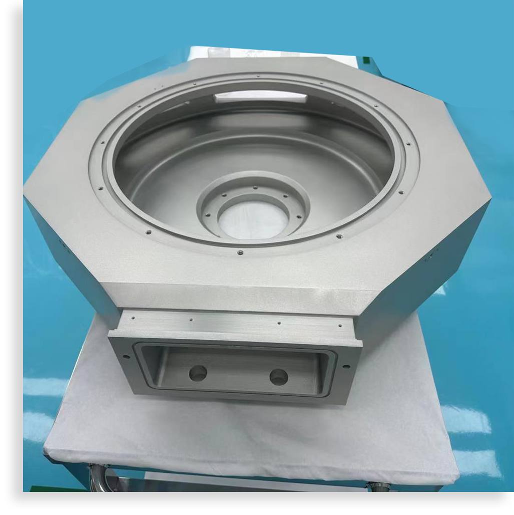
The collaboration between semiconductor chambers and vacuum chambers is a testament to industrial progress. Vacuum chambers create the controlled environment essential for semiconductor processes. By removing air and other gases, they ensure the absence of contaminants and impurities that could compromise the integrity of semiconductor components. This vacuum environment is essential for the following reasons:
Eliminating Contamination: Vacuum chambers prevent unwanted chemical reactions and particulate contamination, ensuring that the semiconductor wafers remain pristine throughout the manufacturing process.
Enhancing Deposition and Etching Precision: In a vacuum, materials can be deposited and etched with unparalleled precision, enabling the creation of smaller and more efficient semiconductor components.
Reducing Oxidation: The absence of oxygen in a vacuum prevents oxidation, which can degrade the quality of semiconductor materials over time.
Optimizing Process Efficiency: Vacuum conditions allow for better control of temperature, pressure, and gas flow, leading to improved process efficiency and repeatability.
Applications and Advancements
The integration of semiconductor and vacuum chambers has led to remarkable advancements in semiconductor manufacturing:
Miniaturization: The semiconductor industry’s relentless pursuit of miniaturization has been made possible by the precision and control offered by these chambers. As a result, we enjoy ever-smaller, more powerful electronic devices.
Energy Efficiency: Advanced semiconductor chambers have enabled the development of energy-efficient electronics, contributing to reduced power consumption and extended battery life in our devices.
Quantum Technologies: Quantum computing and other quantum technologies are now feasible due to the extreme precision and ultra-pure conditions provided by these chambers.
AI and Data Processing: The semiconductor-vacuum chamber synergy has empowered the growth of artificial intelligence and data processing, revolutionizing industries and scientific research.
In conclusion, the marriage of semiconductor and vacuum chambers exemplifies the incredible strides the industrial sector has taken in advancing technology and reshaping our world.In this article, we’ve explored the critical role of semiconductor and vacuum chambers in industrial progress.
If you require such products, please don’t hesitate to reach out to us via email for personalized solutions.
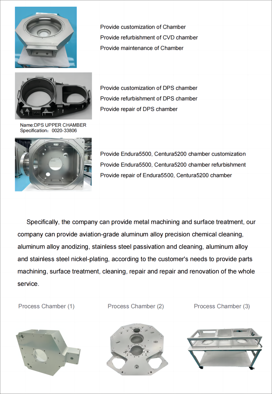
Specifically, the company can provide metal processing and surface treatment, if you have other types of chamber’s products, please contact our company: sales820@xy-global.com